Search This Blog

Friday, 11 December 2020

Reverse Engineering at -17V and 200kHz


Warning: Rabbit Holes ahead


I have a Rockwell 920/3 calculator.


It's from about 1975, and is a pretty impressive beast. It's programmable and has 960 steps in its fully expanded form, a printer and a magnetic card reader/writer as well as a sixteen digit display. It can store data on cards as well as programs. The one I have (well the first one I got) ran the payroll at a large catalogue company in the UK. 

The card reader didn't work when I got it, which was a shame. I had several cards which had programs on them and I wanted to get them off the cards somehow. When a second calculator came up for sale I bought it. I swapped the card reader into my first machine and it worked. If you want to see it working there's a video here: 


I printed the programs and will look at transcribing them later. Of course when a third machine came up for sale I bought that as well. It turned out to be a 920/2 rather than a 920/3, which was a variant with less memory than the /3, but more than the base /1 model. Internally the machines have a common base board which comes with a small amount of RAM. This is one of them with some of my debug connections attached.


The architecture of the calculator is really what we would call a single board computer. There's a processor, RAM and ROM together with some general purpose IO (GPIO) devices. The processor is an early one, the Rockwell PPS-4, a four bit processor used in quite a few devices in the 1970s, notably calculators and pinball machines. It runs from a pretty non-standard, at least these days, -17V supply. It's negative logic so a zero is -17V and a one is 0V. Not something that can easily be attached to my logic analyser or even oscilloscope. The clock rate is one you don't see a lot these days: 200kHz. The second and third machines don't run at the moment, so I decided to have a go at fixing them. As it would be useful to know what the code was doing I decided to instrument the bus signals with a view to watching code execute and also hopefully build up a ROM dump. I could desolder the devices (all of which are in an uncommon 42 pin staggered QIP package) but then I'd need a ROM dump machine that runs at -17V. I may build one of these later if I can't dump all the ROM by bus capture on a working machine. If I run the machine through all of it's features while I have a scanner attached I should be able to slowly capture the contents of ROM. The executed parts anyway. i made a test circuit to see if I could get something working at -17V, the result is in this video:


That worked well, so I went on and made a PCB with enough inputs that I can capture the relevant signals to allow code execution flow to be examined. It turned out that a simple (and cheap, useful if I make a mistake at -17V) blue pill (STM32F103C8) had just enough GPIOs to handle the address bus (A/B in PPS-4 speak), data bus (or I/D bus), and bus control signals.

A datasheet for the PPS-4 is available on the web, and I found some example code in a patent. That gives me something to test my disassembler and any object code I find against as a sanity check. I f you look at the processor bus you find it is a bit of a monster, at least compared with something like the Z80. It is a multiplexed, interleaved two phase type of thing. There are four clock phases (my terminology). ROM addresses come out on the address bus in phase 1 while RAM or IO data is on the data bus. Then in phase 3 the RAM or IO address comes out on the address bus while the ROM data is on the data bus. This diagram from the datasheet should make things clearer:

No? If you look at it for about 10 minutes it starts to make sense. Yes, the processor has two clock inputs, at two frequencies and slightly out of phase with each other. There's a special IC just to generate these clock signals. You can see that de-soldering the ROM chips to read them is the easy bit. Once de-soldered you have to dump the ROMs using this bus arrangement, not forgetting that the logic levels are 0V and -17V.

What is useful about the bus scheme is the pair of 'bus clear' phases. It gives a simple handle on the bus phases when looking at traces. You'd have thought that was straightforward, but the PPS-4 throws another spanner in the works by inverting clock B and also inverting some (just some) of the data on the bus before it is used. Sometimes it inverts a nibble, sometimes a byte. A blank phase is a piece of driftwood to cling on to.

After some simple tests with the blue pill I ended up with a sketch that capture the bus signals as fast as it can manage. I added a pretrigger delay of a number of clock cycles from the reset signal going inactive so that the window of captured bus signals can be moved about with the aim of capturing the inital code execution. Hopefully this will provide some insight into why the board does not work.

 The bus traces look like this:

A:000 D:04 CLKA:0 CLKB:1 WOL:0 DO:0  - 0
A:000 D:00 CLKA:0 CLKB:1 WOL:0 DO:0  - 1
A:000 D:00 CLKA:0 CLKB:1 WOL:0 DO:0  - 2
A:000 D:00 CLKA:0 CLKB:1 WOL:0 DO:0  - 3

A:003 D:00 CLKA:0 CLKB:0 WOL:0 DO:0  - 0
A:003 D:00 CLKA:0 CLKB:0 WOL:0 DO:0  - 1
A:003 D:07 CLKA:1 CLKB:0 WOL:0 DO:0  - 2

A:000 D:0F CLKA:1 CLKB:1 WOL:0 DO:0  - 0
A:000 D:00 CLKA:1 CLKB:1 WOL:0 DO:0  - 1
A:000 D:00 CLKA:1 CLKB:1 WOL:0 DO:0  - 2
A:000 D:00 CLKA:1 CLKB:1 WOL:0 DO:0  - 3

A:003 D:1C CLKA:1 CLKB:0 WOL:0 DO:0  - 0
A:FFF D:1C CLKA:1 CLKB:0 WOL:0 DO:0  - 1 1C
A:FFF D:1C CLKA:1 CLKB:0 WOL:0 DO:0  - 2
A:6AB D:1C CLKA:0 CLKB:0 WOL:0 DO:0  - 3


You an see address 3 in the second block, that's a ROM address, and then in the fourth block the data from the ROM is put on the bus. The contents of the data bus when the ROM address is presented is the RAM or IO data from a previous IO or read instruction.

The captured data is copied to text files, one per pretrigger 'window'. A series of scripts extract the ROM information. This is sparse data, as obviously only ROM addresses that are either executed or accessed by instructions is captured. One key sequence is the startup code:

000     0x81       t 0x1
001     0x82       t 0x2
002     0x74       ldi 0xB
003     0x1C       iol 0x1E  
005     0x7E       ldi 0x1
006     0x1C       iol 0x1D  

The processor starts at address 000 when reset, so we have a sensible trace. The next instruction is a jump (t : transfer) from address 000 to address 001. This is a bit odd, but sort of makes sense. Then there's a jump from address 001 to address 002. Again, odd, but maybe the processor has to do some setup in the first instruction cycles, or the program counter gets 'finalised' or something by doing this. I did find some PPS4 code in a patent and the start of that looks like this:

     0000 81        T       #1                                                   
     *SET O/P TO ZERO                                                          
     0001 7F        LDI     0                                                    
     0002 10 0E   IOL     #E                                                   
     0004 7F        LDI     0                                                    
     0005 10 0D   IOL     #D                                                   
     0007 7F        LDI                                                          
     0008 10 07   IOL     1                                                    

There's the same jump instruction at 000, so we have another flag that we have a sensible trace. The second jump from 001 to 002 isn't there, though. I've not found an explanation of why they are there.

The IOL instruction sends a command to one of the GPIO chips. These aren't memory mapped or IO mapped but instead have hardwired device numbers. The IOL 0x1E sends command 0xE to device 1. This is setting up the keyboard/display scanning signals. I have traced enough signals on the PCB to determine the device numbers for the GPIO chips. I've called the PPS4 processor chip a processor up until now, but this isn't quite right. The chip does, in fact, have input and output ports. They aren't GPIO ports as they are fixed inputs or outputs. So the chip is close to being a microcontroller in some ways. The output port is used in the 920 to drive the demultiplexor that drives each display digit. The inputs are used to sense the keyboard matrix (the scan signals for the keyboard are the same scan signals used to drive the display digits).

Instruction Set

I'm familiar with the 8 bit processors, the Z80 and 6502 and the ARM instruction set. I've also programmed in PIC assembly, and Z8, and 6301, and 8086, and 8051, and 4 bit microcontrollers, and so on. But I was still a bit surprised when I saw some of the PPS-4 instruction. They seem to be from a time before people had worked out the rules. Here's an example, the load immediate instruction:


Ok, it's 4 bit, fair enough, and the immediate value is a nibble in the opcode, fine. Then you see on the right hand side that it refers to a note 3 lower on. Let's look at that:

Ok, so for these instructions (not all instructions), the nibble that is the immediate data is inverted in ROM and hence on the bus. Hmm, a bit odd, but a disassembler or assembler will handle that. Then you notice that a note is mentioned in the fourth box from the left. Is it referring to the same note 3? No it's not, it's this one it is pointing to:


Right, now we have some oddness. If you load the accumulator with 6 and then load it with 4, it ends up with the value 6. This struck me as downright bizarre when I first saw it, but after seeing some code and thinking about it it is useful. If you want to enter a routine with various different parameters then you can do this sort of thing:


Enter6    LDI 6

Enter7    LDI 7

Enter 8   LDI 8

           * Do something with A

          RTN


If you jump to Enter6 then the accumulator is loaded with 6, the next loads are ignored and you do something with 6. If you jump to Enter7 then the accumulator is loaded with 7 and the next load is ignored and you do something with 8. I can see how that could be useful.

This instruction:


shows the use that is made of data tables in ROM at the instruction level.

Next...

I now need to trace the code execution through to the loop it ends up in so I can maybe work out what isn't right... I also need to draw up a schematic. The PCBs are fairly low density so it probably isn't a massive job.


 Memory Expansion

An aside.The 920/2 has one plug-in memory expansion board, the 920/3 has two:


 Rather surprisingly the /2 RAM board has four RAM chips, the /3 boards have six chips each. Another surprise is that the two six chip boards in the /3 are different from each other. It looks to me that the connector pinouts on the cards are different, even though they carry the same amount of RAM. So rather than using the same PCB for both memory expansion configurations (part populating the 920/2 board), there are three different PCBs.


Thursday, 26 November 2020

All This to Get Back Where It Started

 All This to Get Back Where It Started

Storing scrap PCBs is all well and good but what do you do with them? After buying a vacuum desoldering machine (wonderful piece of kit), I decided to dismantle the scrap PCBs that I'd been holding on to for years. One of the PCBs I removed components from was a VCR which had a large vacuum fluorescent display on it:


Underneath the display was a controller chip:


It is a Mitsubishi M50957-199SP. I didn't know what that was, but fortunately there is data on the web about it, and it turns out to be a 6502 micro-controller that goes by the family name of MELP. It's a mask-ROM device (the 199SP denotes the actual code loaded into the ROM) and has several peripheral devices embedded in the package as well as the 6502 processor. It's in a slightly odd 64 pin package with a smaller than 0.1 inch pin pitch. It has built in high voltage drivers for the VFD, which would be nice, if it wasn't mask-ROM based. That is a real show stopper if you want to do anything with these chips. Mitsubishi, though, built in a 'microprocessor mode' which can be set up at reset by pulling a pin high. That then causes the address and data busses to be sent out of what would have been IO ports, together with a couple of control lines (RW and SYNC). That allows the device to run off entirely external memory. OK, we can do something with this device now...

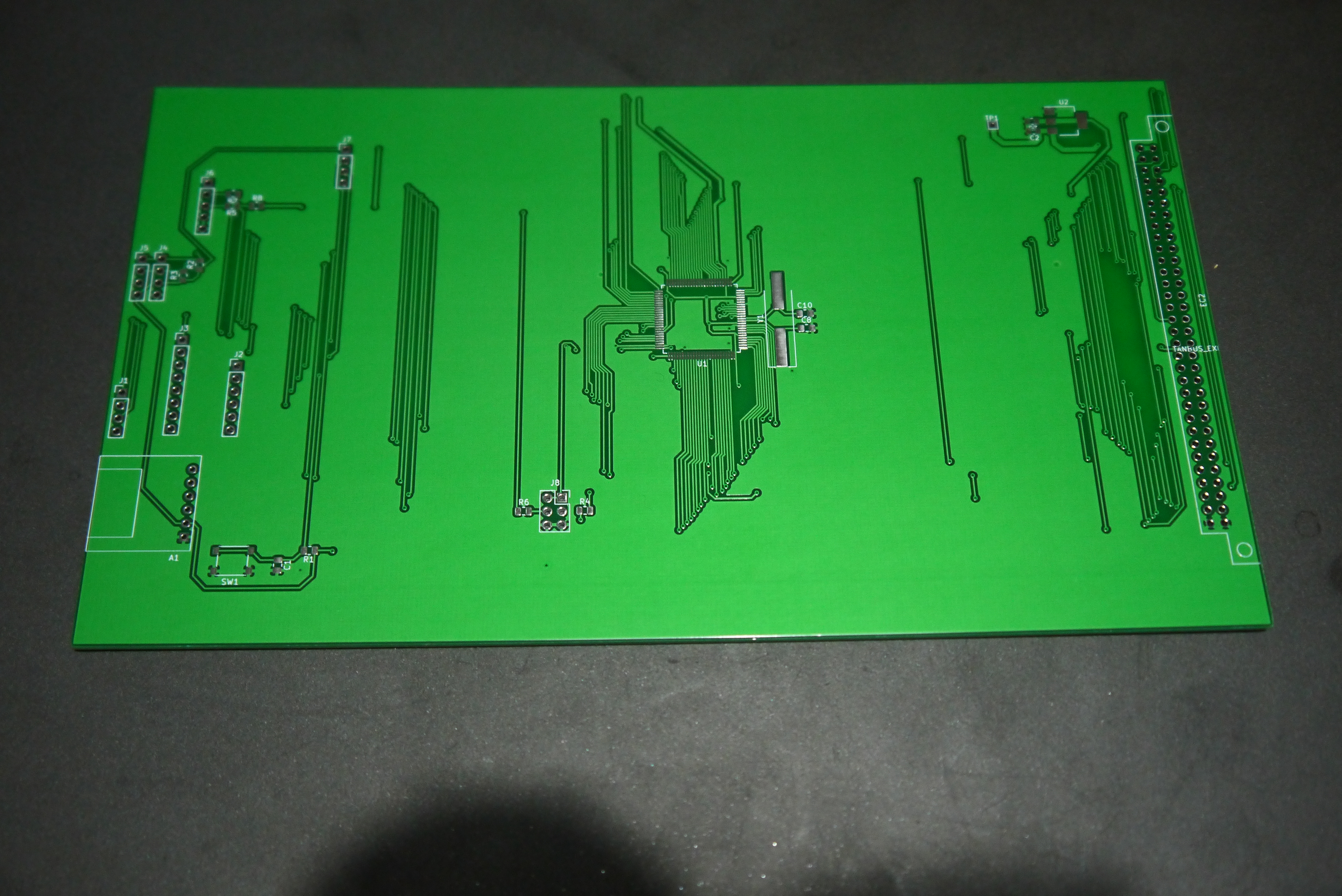
I really only wanted to fiddle with the chip, so started thinking along the lines of a 'trainer' or development board, something like the Sinclair MK14 microprofessor or AIM 65. After a few days of musing and then a couple of weeks of PCB layout I came up with this:


Well, yes, there's two of them. The one of the left is the first populated PCB, and it has the VFD and MELP from the VCR. There's a keypad made from MX style keys, they are much nicer to type on than tactile switches. The VFD requires a high voltage to run, so there's a DC-DC converter for that. The VFD filament requires a driver circuit so I included that, but ended up just using 3V3 on this VFD. The high voltage is switched to the VFD using two MAX6921 driver chips. There's an SD card reader for storing programs and an OLED display for extra information when a VFD is fitted and as the only display if a VFD isn't fitted. I only have one of these VFDs, after all. The VFD is mounted on a plug-in adaptor board (perfboard here) so in theory you could attach a completely different VFD if you had one. 

The whole thing is pulled together with an ARM STM32H742, which attaches to the external address and data bus of the MELP and emulates external ROM and RAM (I suppose it actually only emulates RAM, but the MELP doesn't know that). This ARM is a bit of a beast, it runs at 480MHz, has 2MB of flash and 1MB of RAM. It was a bit of a pain to get going as it doesn't have very good (or indeed any) support in the Arduino IDE. I ended up adding my own board definition to the IDE for this PCB. It's odd that there's no generic STM32H7xx board as there is for the STM32Fxxx devices. I suppose they are more common due to the blue pills. This device is also quite pricey, at about £9 each. I noticed the price when I inadvertently ran one chip at 5V for a few days. It turns out that they will run at 5V, but not for long... Then you have to spend an hour or so desoldering a 100pin QFP before fitting a new one.

The VFD has a lot of segments, and so I had to fit two MAX6921s. 

It means there is plenty of scope for displaying useful information about the address and data buses.

So far I've built some code that drives the 6502 through a short program. This program sets some configuration bits and then dumps memory to a fixed address. I wanted to see if I could change the MELP mode to one that would allow access to the mask ROM within the device, but it does look like the internal ROM is not accessible in any mode that 'microprocessor mode' can access.

The code does, however, drive the MELP and supply data from emulated memory when it needs to. You can see the program running in this video:


As I had five PCBs I had a look on eBay for more MELP chips, and did find some. They are slightly different, M50959-133SP, which has more on-board RAM and a different mask ROM. They do work though, so I have enough for the other PCBs.

I can also use this PCB to test VFDs as it has segment/digit drivers and a high voltage adjustable supply and a filament driver. All I need to do is make an adaptor board for each different display type.

As well as a trainer for the 6502/MELP, I'm thinking of adding code that allows this to be an ARM trainer as well. It's probably not going to be as simple to look at ARM peripherals and do a spot of machine code programming as the 6502, but could be fun fiddling with a 480MHz processor at machine code level. The SD card reader means that you don't lose anything you've done, and you can even build large programs on a PC then transfer it over on a card.


Friday, 30 October 2020

Is This the Past, or the Future?

We have a rainwater harvesting system, which comprises a large tank in the garden fed by rainwater, a submerged pump in the tank and a pump controller in a cupboard in the kitchen. Yesterday our washing machine that is fed from the rainwater had it's red 'Check input' light on. Not good. What was even less good was the water that had been squirted up onto the roof of the cupboard. The problem was a diaphragm that is used, I believe, in a pressure switch that the controller uses to determine that it has pumped enough and should switch the pump off. It had split, allowing water into the expansion chamber above it and out of an air bleed hole. 


You can just see the split on the front left of the diaphragm. Well, the obvious thing to do is to get a replacement part. A lot of the time this is not possible, because they are unobtainable or the unit is obsolete and parts are not available any more. Well, I was quite surprised when I found out that this part is indeed available (and in stock). That's mildly unusual, but what makes it more unusual is that my controller is now superseded by another unit. That unit uses an identical diaphragm. The new controller also uses a new lower power controller, but it has been designed with the same footprint and mounting as the old one, so it can be used in the old controller housing. I've not seen this level of parts interchangeability much, maybe not at all.  It means that the design of the new controller has seemingly foregone extra profit from people having to replace controller units in favour of allowing repair and replacement of parts.

This isn't the first problem I've had, a while back a capacitor failed, and I replaced it:

 https://trochilidae.blogspot.com/2018/02/rainwater-harvesting-pump-controller.html


Another surprise that happened during that repair was that the controller was built from standard ICs and components. It is not a microcontroller based design. There is no firmware. If the controller PCB fails it is possible to repair it or even make a new PCB. This controller appears to be repairable for quite some time to come. 

So is this a design from the past, where almost everything was repairable and electrical and electronic equipment even came with circuit diagrams? Or is it a design from the future that uses the minimum disposable parts and doesn't have built-in obsolescence?

Either way, I like it.

Wednesday, 28 October 2020

Sharp PC-G850VS PIC programmer

Sharp PC-G850VS PIC Programmer

The PC-G850VS is a remarkable pocket computer that was only ever sold in Japan. 


One of the features that make it so interesting is a built-in PIC assembler. This can be used to assemble programs for the PIC16F84 or PIC16F84A.  Just assembling code isn't that much fun though, but fortunately you can attach a programming PCB to the 11 pin connector. The PC-G850VS has built-in PIC programming code to match the assembler. There's a design or two on the internet and I designed a PCB around one of them. I added series resistors to the PIO lines as protection and fiddled with the zener diode values but otherwise the circuit was the one I found.


Microtan Arduino Card

Microtan Arduino Card Part 1

The rack mounted Microtan system has the useful feature that it is, well, rack mounted. This means you can attach anything to it by building a card. After building the cassette interface PCB that uses a serial data connection to save and load data, I was wondering if there was a better way to load and save programs from the Microtan. One that was faster and could maybe read and write directly from and to the SD card without using an intermediate RAM buffer. I could use RS232 and handshaking (might try that sometime), but it's still serial. then I wondered about DMA on the bus. Could I build a card that read and wrote directly to and from memory? The TANBUS does have signals that allow DMA access, so it should be possible. There's a block of memory on the Microtan 65 that isn't accessible, but everything else is. What would do the accesses? Well, why not an Arduino Mega? It runs off 5V and has plenty of GPIOs. With DMA it doesn't have to buffer much data as it can do direct reads and writes to the card. It could also maybe monitor the bus and do bus capture traces. It's not got a very fast processor at 18MHz, but the Tanbus is only 750kHz, so it might be possible to capture traces in code.

It was worth an experiment, so I made some PCBs that had a Mega Pro embedded on a card that fitted in the rack.


Once populated I ran  some simple code to sample the bus asynchronously. This appeared:

Microtan 65 DMA Gadget

00: FE03-FF  FE04-7F  FE01-0C  FE05-FF  FE07-FF  FE03-FF  0004-FE  FE05-0C 
08: FE06-FF  FE07-FF  FE03-FF  0001-FF  FE05-FF  FE06-FF  FE07-FF  FE04-FF 
10: 0001-71  FE05-FF  FE06-FF  FE03-FF  FE04-FF  FE01-7F  FE05-FF  FE07-FF 
18: FE03-FF  0004-FF  FE05-DF  FE06-FF  FE07-FF  FE03-FF  0001-6E  FE05-FF 
20: FE06-FF  FE07-FF  FE04-FF  0001-00  FE05-FF  FE06-FF  FE03-FF  FE04-7F 
28: FE01-04  FE06-FF  FE07-FF  FE03-FF  0004-FE  FE05-00  FE06-FE  FE07-FF 
30: FE03-FF  0001-FF  FE05-FF  FE06-FF  FE07-FF  FE04-FF  0001-01  FE05-FF 
38: FE06-FF  FE03-FF  FE04-FF  FE01-FF  FE06-FF  FE07-FF  FE03-FF  0004-FF 
40: FE05-9F  FE06-FF  FE07-FF  FE03-FF  0001-FE  FE05-FF  FE06-FF  FE07-FF 
48: FE04-FF  0001-04  FE05-FF  FE07-FF  FE03-FF  0204-FE  FE01-04  FE06-FF 
50: FE07-FF  FE03-FF  0004-FE  FE05-00  FE06-FF  FE07-FF  FE03-FF  0001-FE 
58: FE05-FF  FE06-FF  FE03-FF  FE04-FF  0001-09  FE05-FF  FE07-FF  FE03-FF 
60: 0004-FF  FE01-DF  FE06-FF  FE07-FF  FE03-FF  0004-6F  FE05-87  FE06-FF 
68: FE07-FF  FE03-FF  0001-FF  FE05-FF  FE06-FF  FE03-FF  FE04-FF  0001-00 
70: FE05-FF  FE07-FF  FE03-FF  0004-7E  FE01-00  FE06-FF  FE07-FF  FE03-FF 
78: 0004-FF  FE05-01  FE06-FF  FE07-FF  FE04-FF  0001-00  FE05-FF  FE06-FF 
80: FE03-FF  FE04-FF  FE01-09  FE05-FF  FE07-FF  FE03-FF  0004-FF  FE01-FF 
88: FE06-FF  FE07-FF  FE03-FF  0004-FF  FE05-0F  FE06-FF  FE07-FF  FE04-FF 
90: 0001-71  FE05-FF  FE06-FF  FE03-FF  FE04-FE  FE01-04  FE05-FF  FE07-FF 
98: FE03-FF  0004-7E  FE01-00  FE06-FF  FE07-FF  FE03-FF  0001-FE  FE05-FF 
A0: FE06-FF  FE07-FF  FE04-FF  0001-C9  FE05-FF  FE06-FF  FE03-FF  FE04-FF 
A8: FE01-09  FE05-FF  FE07-FF  FE03-FF  0004-6F  FE01-FF  FE06-FF  FE07-FF 
B0: FE03-FF  0001-FF  FE05-FF  FE06-FF  FE07-FF  FE04-FF  0001-00  FE05-FF 
B8: FE06-FF  FE03-FF  FE04-FE  FE01-00  FE05-FF  FE07-FF  FE03-FF  0004-FF 
C0: FE05-01  FE06-FF  FE07-FF  FE03-FF  0001-FF  FE05-FF  FE06-FF  FE07-FF 
C8: FE04-FF  0001-51  FE05-FF  FE06-FF  FE03-FF  FE04-FF  FE01-81  FE04-FF 
D0: FE07-FF  FE03-FF  0004-FF  FE05-15  FE06-FF  FE07-FF  FE03-FF  0001-FF 
D8: FE05-FF  FE06-FF  FE07-FF  FE04-FF  0001-00  FE05-FF  FE06-FF  FE03-FF 
E0: FE04-FE  FE01-00  FE06-FF  FE07-FF  FE03-FF  0004-FF  FE05-80  FE06-FF 
E8: FE07-FF  FE03-FF  0001-FF  FE05-FF  FE06-FF  FE07-FF  FE04-FF  0001-19 
F0: FE05-FF  FE07-FF  FE03-FD  FE04-FF  FE01-05  FE06-FF  FE07-FF  FE03-FF 
F8: 0004-FF  FE05-9F  FE06-FF  FE07-FF  FE03-FF  0001-FF  FE05-FF  FE06-FF

The 16 bit numbers are the address bus, and the addresses shown correspond to the POLLKB loop in the TANBUG program. So it seems to work for the addresses. The data bus isn't as good, but that could be because the trace is asynchronous and the data bus doesn't have data on it as long as the address bus does.

I then wrote some code that used the DMA mechanism to read data from memory areas. This stops the processor from accessing the bus and takes over as a bus master. Data can then be read and written as desired.

The principle looks good, but this card has a few problems:

1. It isn't fast enough to capture bus traffic reliably.
2. There's not a lot of RAM on a Mega, so dumping large amounts of the memory space of the Microtan is a problem.
3. I didn't include an SD card, which is a very useful way of getting data into and out of the card and the Microtan

To attempt to overcome these problems a V2.0 card was laid out.


This one uses an STM32F103 with 1Mb of flash and 96Kb of RAM. This is a much more usable size of memory, the RAM allows all of the Microtan memory to be dumped with space to spare, and the large amount of flash allows images to be stored. The processor is much faster too, running at 72MHz. 
The device supply is up to 3V6 so a 3V3 regulator is used and the GPIOs that deal with the bus signals are 5V tolerant. The 5V tolerance is only functional when the GPIOs are set up as inputs, but that is a the normal state while monitoring the bus. When the bus is driven and GPIOs are outputs, however then there could be a problem if the circuitry on the Microtan has a pull-up, for instance. We'll have to see how delicate the STM32F103 chip is when faced with this sort of work.

I've only tried this V2.0 card out briefly and the signs aren't good. I don't think that the ARM processor has been destroyed, but the card doesn't seem to work. I get addresses of 0,1,2,3,0,1,2,3,0,... and the data bus is always 0xFF. It's all a bit too deterministic to be voltage thresholds, well, I think so at the moment. I'll have to investigate...


Saturday, 12 September 2020

Casio CQ-1

 Casio CQ-1

A long time ago, I had a Casio CQ-1. 


It was a weird machine, I suppose, but it was a clock, and a stopwatch, and a calculator, which makes it pretty useful. And the calculator could tell you what day of the week any date was (well, in it's date range). It could calculate the number of days between two dates. And it was an alarm clock.

Not so long ago the batteries leaked and the CQ-1 was binned. This was a shame and I decided to get hold of another one, so bought one on ebay. This didn't turn out too well, as the device would only start up if I held my finger on one of the clock oscillator pins. I tried simulating a finger with various components, but the little chip seemed only happy with my finger. I never found out why, so I bought another CQ-1, hoping to either get enough bits to fix my original CQ-1 or get a unit I could fix. That didn't work out too well either, as it was utterly dead, and no amount of fingering could get it going again.  Aargh!. Third unit and this time all was well. It calculated dates and the stopwatch worked.

At least all was well until I came to use it after a day or two and the AA battery was flat. Aaargh! again. This CQ-1 has a strange fault where the supply that powers the VFD display seems to power up repeatedly even when the unit is off, and that eventually flattens the battery.

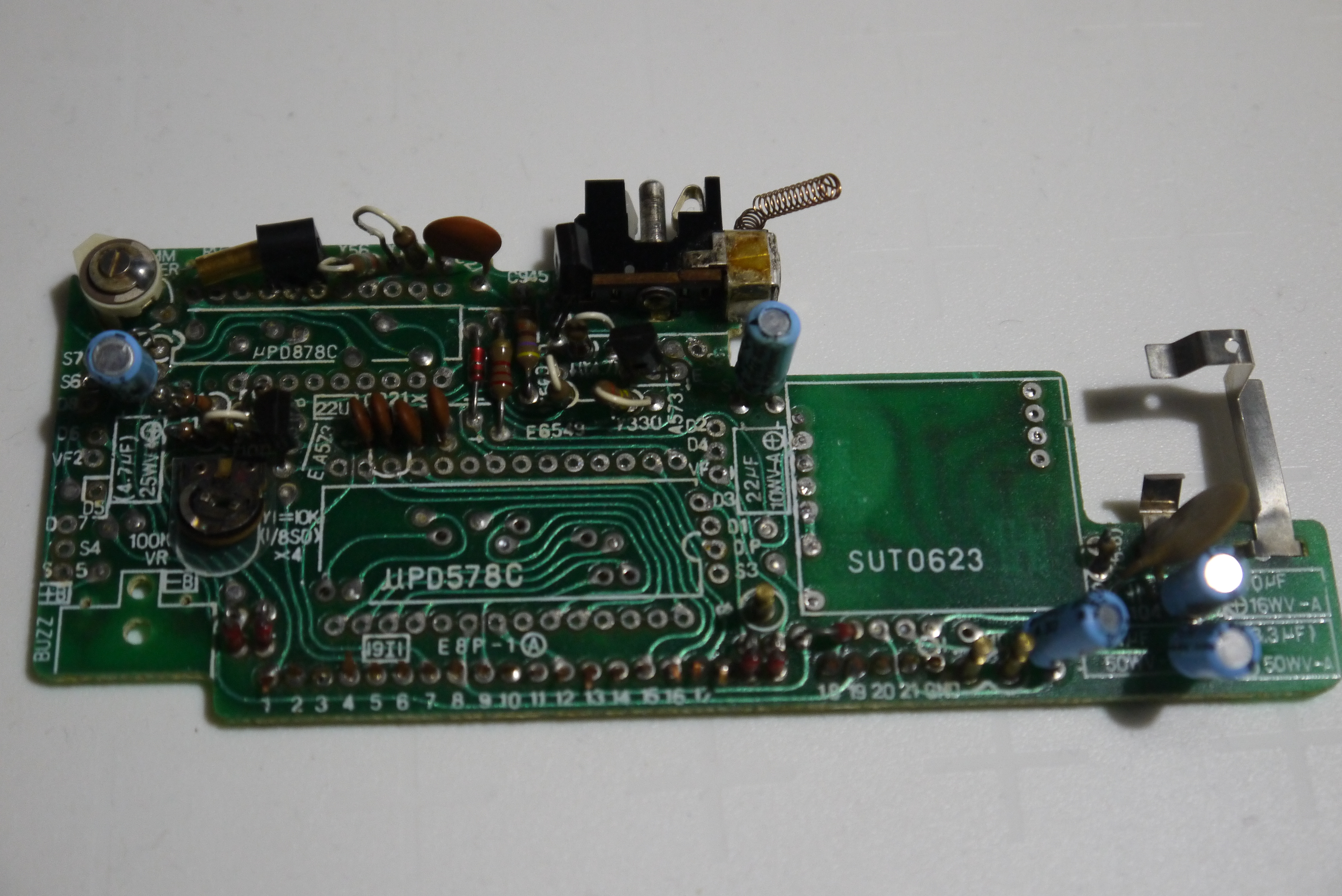
So, I decided to have a go at designing a replacement for the CQ-1 main PCB. This is the one that has the circuitry on it. This is a partially stripped PCB:

It attaches to a keyboard PCB which has one of the AA battery connections on it. The wire tabs connect to two 1.5V watch batteries that power the clock circuit. 

The first attempt at recreation is this:


There's a prototyping PCB (one of Mike Harrison's prototyping boards) with all the circuitry to create the voltages to run the ARM processor (3V3)and the higher voltage needed to run the VFD segments and digits (about 23V). The filament drive is conveniently 3V3 (ac). The PCB is attached to the front half of a CQ-1 which provides the switches and keys. All this circuitry runs off a single AA battery, or USB. As batteries are an evil that has to be tolerated, I did consider running this off just USB, but decided that it was too limiting. i didn't want to use the original CQ-1 PSU as I've never seen one, and USB is just so convenient. I haven't carried over the silver oxide batteries that run the clock, instead the RTC chip runs directly off the battery. It is a low power chip so that's not a problem. If there's 3V3 then it runs off that too, so you can plug a USB cable in when changing the AA battery.

This is a close up of the prototype PCB.


There's a blue pill providing an ARM processor, programmed with an ST-LINK. There's two dc-dc converters, one to go from 1V5 to 3V3 and one to go from 3V3 to 23V (-ish). The 23V supply is switchable from the processor and turns the display on and off. The VFD is driven from a MAX6921 chip which has a serial connection to the processor. The timekeeping is provided by an MCP7940 chip with it's own crystal. This is attached over I2C to the processor. i took a VFD tube from a donor CQ-1 and that is used as the display. The beeper is also from a CQ-1. Due to the STM32F103C8 on the blue pill not having enough GPIOs to handle all this hardware and scan the keypad, a GPIO expander is used on this PCB to provide more GPIOs. This is accessed using I2C.

Of course, this doesn't fit in the original case, so a V2.0 PCB has been created that does:

This is basically the same circuit, but the dc-dc converters are now in component form on the PCB, and the GPIO expander has been dropped as a larger STM32 chip with more GPIOs has been used. This is capable of all the IO and keypad scanning. It also has more flash and RAM (512K of flash and 64K of RAM). As the STM32F103 chips are all very compatible there are a few options for flash and RAM simply by fitting a different variant of the chip.

I've also added the connections for an OLED display on this PCB so if the CQ-1 VFD is broken then you can use a dot matrix OLED display. The 23V dc-dc converter can be left out if the OLED is used, as well.

Here's the first populated PCB in a case:

It fits nicely, the wires coming out are the ST-LINK programmer wires. The USB power goes in through the battery cover latch hole which I filed out so the USB socket was accessible. The circuit should run off a single AA battery as well (the prototype did, but I've not tested the new PCB yet). I'll need to print a connector for the positive terminal of the battery, the negative is a spring on the keypad PCB.

Here's the front side of the PCB:


Again the beeper and VFD tube are from a CQ-1. The keypad PCB is mounted using 0.1" plug and socket connectors, the spacing was perfect, even though the original CQ-1 uses copper strips held together with plastic.

The PCB needs a modification as I got one signal wrong, the keypad connector is out by 0.1" for five connections, the 23V dc-dc converter inductor whistles, and the mounting hole for the beeper is too small, but other than that I'm very happy with it. It fits the case well.

There's a few things left to do. The display is a bit dim, which is probably the 23V dc-dc converter needing to be 26V or so. There's a lot of code to write if this is going to be the same as a CQ-1 but there's a rudimentary stopwatch and integer-only calculator, together with a clock you can't set, but writing the code is the fun bit...

See it working here:


Some pictures of it operating:


The USB cable that is powering it and the programming wires that come off a header on the PCB:


And displaying some characters that the original just can't manage: