It's a Casio FX502P in pretty much perfect cosmetic condition. Unfortunately the display isn't. It's not displaying anything very well at all. It's attempt at displaying Pi shows how bad the LCD is:
Once I opened it up, the problem was immediately obvious. It was battery leakage again. It's not very obvious in this photo but the batteries have leaked in the area of the battery contacts (which are remarkably clean) and the LCD.
The LCD is fortunately connected with zebra strips on this calculator, not heat seal:
This meant that I could dismantle the display and clean it. I also cleaned the tracks that had had leakage on them. the solder resist was loose so I removed it on any affected tracks. You can see that tracks I've cleaned are missing their resist and appear gold in this photo:
Once re-assembled, the LCD is working perfectly. It's got good contrast and the filter is completely free of scratches. It's the best example of a FX502P I've got.
The firmware that runs the Casio FX502P gadget that I recently created has a structure and uses a technique that I though was worth documenting. The gadget uses the Arduino framework and is described in the following videos and blog entry.
The prototype:
This device has some tight timing constraints while performing interactions with a real-time interface. It cannot waste time deciding what to do next as it has a bidirectional synchronous bit stream to attend to at about 200kHz. The processor itself runs at tens of MHz so there's time for several instructions to run between clock edges, but not enough time that the code can perform time consuming operations.
As the protocol isn't officially documented I'd like to be able to change the interface behaviour to add new commands, remove commands and maybe alter some of the existing commands. The code needs to be easy to understand and change.
So, we have two requirements:
A. Code must run fast
B. Code must be easy to understand and not break if altered
These requirements, even if they don't officially declare war on each other, fight against one another. Code that is easy to understand and change isn't usually fast, and code that is fast isn't usually easy to understand or change.
Fast Code
One fast way to respond to inputs is to use interrupts. Something happens and a fragment of code runs. That's the basis of interrupts. If you have something simple then it's relatively easy to implement. A push-button, for instance, is a single input and an interrupt service routine (ISR) that runs when the input is either changed or at a certain logic level. (An interrupt that runs code when an input changes is edge-triggered, one that fires at a certain level is, well, level-triggered).
In the push-button example it's all straightforward. The push-button is pressed, the input changes level and the code runs. Whatever is needed to be done is done and the ISR exits. There are details that have to be attended to, such as using the volatile keyword (in C), we are more interested in the overall structure here than details.
For the FX502P gadget the interface has:
A clock line that runs at approximately 200kHz and clocks data on both edges
A data line, which is bidirectional
Two control lines, active high
A serial data format that uses packets of different lengths, including a longer packet that has a payload with start bit, stop bits,data and parity, which also gets clocked out on a different edge to the data clocked in.
We therefore have edge triggered signals, level triggered signals and have to collect and build packets of different lengths and formats. Suddenly it's all a lot more complicated than a push-button.
At the time of writing (and as this code is easy to change, it changes now and again), there are two interrupts, one driven from the clock and one from a chip enable (CE) control line. The complexity has just moved up a notch. There's now two interrupts that have to be handled. Fortunately in this case they cannot execute simultaneously, although the method I have used doesn't have problems if they do execute simultaneously (on different cores, for example).
Orchestration
So how can you create something that can react to interrupts and perform actions based on those interrupts? Not only react, but react in a way that has memory of what has happened in the past. For instance, if the clock changes state do we clock data in or out? We need to know if we are in the middle of receiving a packet or sending one.
In the gadget this is done with a Finite State Machine (FSM). It's a thing (Machine) that can be in one of a Finite number of States at any time. FSMs move between states when they receive an input (stimulus). (An FSM is always in a state, and changing from one state to another logically takes no time). There are many ways an FSM can drive outputs, in the one used here, a function is called when the FSMmoves to a new state. An action is taken on entry to a state.
When an ISR runs, it sends a stimulus to the FSM and that may causes a state change. Code is run when entering a new state, that code can do anything required at that time.
Implementation
There are several ways to implement an FSM. As the gadget doesn't have time to spare it uses nested switch statements. You can use a table driven approach but searching the table uses processor cycles and hence more time than a switch statement approach. Using a table, though, allows you to use a higher level of abstraction when defining the FSM. With the gadget I wanted a similar abstraction, but to achieve this I used what I call a 'software hammer'. The idea is to have an abstract description of what you want to achieve, in a form that is easy to understand and easy to alter, and support code that hides the details. This support code is 'hammered' into shape to support the abstract code and handle all the details.
In the gadget code, the nested switch FSM is the abstract part, the rest of the code is hammered to support that abstraction.
Here's a fragment of the FSM code which shows the two nested switch statements:
switch(ce_isr_state) { case CIS_IDLE: switch(captured_word) { // Close followed by reset is a '.' key case IP_CLOSE: ce_isr_state = CIS_POSSIBLE_DOT; break; case IP_RESET: ce_isr_state = CIS_POSSIBLE_AC; break; case IP_UNKA: ce_isr_state = CIS_RX_UNKNOWN_A; break;
The first switch decides which state the FSM is in, the second is one which looks at the word that has been captured by the support code in the ISRs. Depending on the value of the packet, the FSM is moved to a new state.
For example, if we are in the IDLE state and we receive a CLOSE packet, then we move to the POSSIBLE_DOT state. It's pretty easy to see how the states follow the packets received from this fragfment, and altering this code is not tricky at all.
The first fragment covered receiving packets and deciding what to do, based on the contents. What about sending data? here's a fragment from a state that needs to send data:
case IP_WAIT:
ce_isr_state = CIS_RX_WAIT;
num_data_words = 0;
// We want to send a 0 bit on the next clock cycle,
// set it up
isr_send_data = 0;
isr_send_data_save = isr_send_data;
isr_send_bits = 1;
isr_send_bits_save = 1;
isr_send_flag = true;
SET_DATA_BIT0;
break;
This is run when the WAIT packet has been received. The required action is to send a packet back of length 1 with the value 0. It's pretty easy to read:
isr_send_data = 0;
sets up the data to send while:
isr_send_bits = 1;
sets up the length of the packet.
Then:
isr_send_flag = true;
indicates to the support code that a transmission is needed.
There's some other housekeeping stuff, because the universe requires it, such as the SET_DATA_BIT0 which is exposed here due to the timing of the interface. It can't be done later.
What is important is that the fact that the received data packets are clocked in on one edge of the clock while the transmitted packets are clocked out on the other edge is completely hidden at this layer of abstraction. That detail has been hammered into the support code.
Even though the details of the support code are probably horrible with lots of special case required by the interface, that doesn't matter once it works, as from then on it should only be necessary to change the abstract code when new packets need to be decoded or transmitted. The support code handles the interface, and that isn't going to change.
The whole of the FSM looks pretty much like these two pieces of code, although there are other things that need to be done, like this:
case CIS_WAIT_DATA: if(word_bits == 16) { // 16 bits of data // If data is all 1s then it is header data if( (captured_word & 0xFFF0) == 0xFFF0 ) { // Header word, ignore it // Back for more data num_header_words++; // We know the length of the next packet isr_hint_length = 6; ce_isr_state = CIS_WAIT_2; } else { // Store this data data_words[num_data_words++] = captured_word;
Notes
FSM State
The state an FSM is in is determined by it's state variable. Whatever number is in that variable is the state it is in. It can't be in two states at once and it take no time (logically) to update a variable's value.
DFSM
These FSMs are actually DFSMs (Deterministic Finite State Machines), which means that the state transitions are deterministic. Non deterministic state machines can also be useful, their state transitions can be random in some way. They are not that common, though.
Race Conditions
FSMs can be resilient against race conditions. If stimulii are queued and then processed then you can build your FSM to handle stimulii in any order and still get the correct behaviour. Every state should be examined to see what action it should take for every possible stimulus. It doesn't matter when or in what order the stimulii arrive, the FSM states will always take the appropriate action, and it won't miss stimulii as long as the queuing code is correct.
It decoded the frequencies that the FA-1 sent to a cassette recorder and wrote the data to an SD card attached to an Arduino Due. I had to use a Due as it was the only combination of clock frequency and RAM that could keep up with the data stream coming out of the FA-1.
The advantage of using this approach was that the cassette interface was a well-known format and fairly easy to decode. The disadvantage is the bulk of the final package. To get the data onto the tiny little SD card you need the FA-1 cradle and the gadget. A few weeks ago I suddenly realised that I could cut down on a lot of the hardware needed by attaching a gadget to the expansion port on the top of the FX-502P. This would involve interacting with the protocol that goes over the expansion port, but that shouldn't be a problem. There's a lot of detail here about the expansion port of the FX-602P and FX-700P.
As a base for a prototype I used the Sharp PC-G850 gadget, using the Blue Pill processor and the OLED display. The expansion port signals are attached to the 11 pin Sharp interface connector on the gadget using a cable.
The protocol that the expansion port uses is a bit odd. It seems to be the bus that the processor in the calculator uses to talk to the LCD controller. It has a single bi-directional serial data line, a chip select, a command/data control line and a clock for the serial data. The data packets are of variable length, which makes it a bit hard to decode. Most packets are 6 bits long, there is one two bit packet and a 16 bit long data packet (holding an RS232 type character format that encodes a single byte of data. The clock edge that the data is latched on is different for transmitted and received data. And the data is inverted logic (0 is 3V and 1 is 0V, not forgetting that the calculator uses 3V as it's 'GND' and -3V as its VDD).
Once the signal levels are sorted (use 0 and 3V to power the STM32, invert data to get levels that match the known commands for the FX-602P) the data and clock can be fed to GPIO lines on the STM32, The bus runs at around 200kHz, so there's not a lot of time to process the packets. It is not feasible to have any delays so I run the decoding code purely in interrupts (one on the SP or clock line and one on the CE signal). The timing is so tight that initially I had problems with the serial port disabling interrupts (I presume that is what it was, disabling serial IO removed the problem), those problems went away with later code, but I can still disable the serial port access when packets are received.
The data that is sent and received is held in a RAM buffer, there is no time for access of the SD card, so the RAM buffer is stored and loaded from SD card when needed.
After quite a lot of reverse engineering of the interface (the FX-502P is not quite the same as the FX-602P) including capturing traces of communication between the calculator and an FA-1 adapter, I got some working code that could both send and receive data files from the calculator.
This gives a gateway between the calculator and the outside world. The calculator has a limited number of ways to send information over the interface. It can send or receive a single number (this is the quickest transfer), it can send or receive all memories
At this point the prototype was limiting the code as there isn't sufficient flash memory on a Blue Pill (STM32F103C8) to implement the features I wanted to add. The basic idea had been proven with the prototype, time to move on to a better platform. For that I chose the STM32F103RE device. Or, more accurately I chose the 64 pin QFP package. The STM32F103 family has nice pin compatible genetics, so several devices of different capacities will fit onto a particular footprint. Using the 64 pin QFP I can got up to 1M of flash and 96K of RAM down to 16K of flash and 6K of RAM. There's also a lot of GPIO on this package, way more than I need for this gadget.
It has a small 0.96" OLED display, an SD card module and a programming header that uses an STLINk V2. It also has a serial data header with TX and RX, and a header with 8 GPIOs on it (and power):
The PCB plugs into the connector on the top of the calculator. Optionally the PCB can supply power to the calculator, or it can run off batteries, there's a jumper for that. It's the red one.
I have also used a USB socket breakout board for the USB connection, which supplies poiwer for the PCB and also provides a serial connection. I use a breakout board as the USB sockets have a habit of ripping off the PCBs and taking tracks with them. This way the tracks are on a disposable PCB, not the more valuable one. I've already replaced the USB socket and breakout board on the is PCB...
The code is based on the Arduino platform, so it can connect to the serial monitor of the IDE.
What can it do? Well, it can save and load programs and memories to and from the SD card, that's the basic function. It also uses several 'special' values to do other things. Things like displaying programs on the OLED display:
With GPIO lines you can interface any I2C device, such as a real time clock. This is the STM32 displaying time in a display mode set up by the 502, using a DS3231 RTC module:
You can also read the time (and date) into calculator memories:
Of course, it is useful to be able to print things out now and again. Interfacing a simple thermal printer isn't difficult. The one I used accepts serial data so I attached it to the serial data header .The calculator can set up a print flag that sends programs and memories to the printer as well as SD card.
This printer does require a 2A supply, so can't run off the USB direct from the PCB.
There was a printer that attached to the FX-502P, but it used magic metallised paper which is pretty much impossible to find these days, so a thermal paper option is a nice alternative. See here for more magic metallised paper experiments:
As well as the RTC, I've attached a sensor module and an accelerometer, but haven't done much with them other than read registers. There's also a text mode where the calculator has a text screen that it can place ASCII text on, and a graphics screen that it can place pixels on.
More information on these videos.
The gadget should work perfectly fine with an FX-501P, as it's the same code and hardware in the calculator as shown in this video:
The FX-602P and FX-601P use the same interface but a slightly different command set. It should be possible to get it to work, though, with some changes to the firmware on the gadget.
The FX-702P tantalisingly uses the same connector as the 502/602 series calculators, and the same command set as the FX-602P, but unfortunately uses 5V signalling rather than the 3V of the 502/602. The pins used on the STM32 for the calculator interface are 5V tolerant, but there's a couple of issues. The first is that the STM32 should be able to sense the 5V logic levels correctly, but may have trouble driving 5V levels due to 5V tolerant pins still driving at 3V3. The second issue is that the data line is bi-directional and the 5V tolerance on STM32 devices only works when it is configured as an input. I have serial resistors on the calculator interface lines, which might help, but if there's a time when driving the interface that I drive the data line as an output and the calculator does the same then there could be problems. I may try this in the future, as it may work.
Saturday, 11 January 2020
More Magic Metallised Paper Experiments
I've been trying to make paper that works in the Casio FP-10 printer. See the previous post for attempts one to six:
Anyway, I was watching an episode of Wheeler Dealers and Edd mentioned that you use a conductive spray primer before you spot weld, sometimes. That was interesting as I had been looking for conductive spray paint. A quick google and it appeared that yes, this primer was indeed conductive due to either zinc or copper in the spray. Not only that but it as available at a local auto supply shop.
One trip to the shop later and I had a can of pretty expensive zinc spray paint. It was no problem to then spray a sheet of A4 paper:
When dry the surface is similar to the magic paper, and even shines up a bit if you rub the surface:
Unfortunately, even though I did measure some conductivity when drying, the paint seemed to not be conductive when dry. I did a couple of sheets with varying numbers of layers and ran some test strips through the printer:
As you can see, it's a bit messy and clogged the print head as the final product is quite thick. It also didn't work.
Attempt 6b
I then had an idea about testing the paper. I set up a PSU with 15V on it and attached one wire to the paper then dragged the other wire across the paper. This gave me an idea whether the paper would spark erode or not. The real Casio paper worked fine (as expected), but the only paper from my tests that worked was the 'gilded' aluminium one. Here's some scribbles I made, which are spark eroded. The black you can see is some paint I sprayed under the aluminium, just like the real paper.
Even though this manual test worked, it didn't print in the FP-10.
Saturday, 7 December 2019
Magic Metal Paper
In the seventies, Casio created the FP-10 printer for the fx-602p.
It could also be used on other calculators like the fx-502p and fx-702p. Like the ZX Spectrum printer it was a spark printer that used metallised paper. This paper is no longer available, at least anywhere I can find. I managed to get a printer for a reasonable price, and it came with one roll of paper. The paper appears to be a layer of metal at the front (aluminium I assume), then a black layer of some kind and then a paper backing. The rolls are very narrow and only a couple of metres or so long. I only have one roll of paper so I decided to see if I could make some paper to use on the printer.
I measured the paper and got a figure of around 3 to 6 ohms per square (very rough measure).
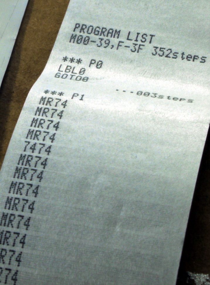
That's a printout from an fx502p, which doesn't ordinarily have any real alphanumeric capability, but the printout does. The printout is very clear.
Attempt One
Aluminium foil. I tried aluminium foil in the printer. This didn't work as the foil doesn't have the physical strength to get driven through the mechanism.
Attempt Two
Stiffen it up. I glued foil to paper to try to give it a bit of stiffness. This also didn't work. The foil tore and I suspect there was no electrical contact between the foil and the metal plate at the front that forms a circuit between the paper and the electronics.
Attempt Three
Try to find conductive paint to spray on some paper. There are conductive paints but they are very very expensive and I didn't try those. I also inquired about silver spray paint that looked like it was conductive. There's no metal in it apparently and it is not conductive.
Attempt Four
I find that there is a conductive paper available. It's called 'teledeltos' and it is used for science experiments and I believe was also used in fax machines many years ago. I bought some (not cheap) and it arrived as a large roll. It appears to be totally unsuitable as it is carbon based and the conductive side of the paper is the wrong side to work in the printer. The resistance of this paper is probably too high anyway at 2000-3000 ohms.
The black side is conductive, but you'd want to print on the white, non conductive side to get contrast. I tried scraping some of the white off so there's contact with the metal plate on the front of the printer, but no sparks at all.
Attempt Five
I tried shiny aluminiumized paper based on a plastic sheet backing. This was conductive on one side but again wouldn't print.
Attempt Six
This involved aluminium 'gilding' foil. This is very thin foil that you can glue to paper (or other surfaces). It results in a shiny silvery effect. I used spray glue to attach the foil to paper as it will not adhere on it's own.
When I measured the gilded paper I got a figure around 0-1 ohms so this is much more in the ball park of the original paper. When I cut strips and ran them through the printer, there were some sparks, but not enough to get a printout.
I'm not sure why not as the resistance seems similar to the original paper. The texture is different though, with the original paper a grey matt surface and the gilded paper much shinier.
Here's a selection of papers that I tried:
That's gilded paper on the left, shiny aluminiumized paper in the middle and the magic original paper on the right.
I also cut some original paper at a shallow angle so the layers become more apparent:
You can see the backing layer of paper, then a black layer and finally the aluminium on top. The black provides a contrast after the metal has been sparked away, I think.
Conclusion
There must be some magic employed in the original paper. It's not just that it is conductive, as none of these conductive 'papers' worked at all. The things I can think of are maybe:
The resistance of the paper is critical to operation. None of the resistances were exactly what the original paper showed, either much higher or slightly lower.
The texture of the paper is important. The original paper has a distinctive matt finish. If you scratch it with your fingernail then you get a metallic shine, so there's aluminium there.
The thickness of the paper is critical. I doubt the papers I made are exactly the same thickness as the original.
The printer has been finely tuned to print on just the original paper. maybe it can be re-tuned to print on other 'papers'.
I'm not sure what to do next. I may have a look inside the printer and see if there's some clues in there.
The Casio fx502p is an old calculator. It is from the 80s which was a time when the cassette recorder was more common that it is these days, and it was used for non volatile storage on devices like this. I have a couple of these calculators, but I don't have a cassette recorder any more, and I really would like to have a better way to store programs than a cassette tape.
So, the MK I cassette interface based on an Arduino Uno:
This breadboarded circuit was capable of reading a cassette file sent by the calculator and then sending that same file back again. The output from the cassette interface is a microphone signal of about 10mV so there's an amplifier stage to get the signal to a logic level. This breadboard proof of concept worked well, so I made a PCB version of the amplifier circuit.
The Arduino Uno is just fast enough to handle the signals from the fx502P, which are 2400Hz and 1200Hz pulses, but I wanted to try to get this circuit working with calculators and computers that use faster signals, so I replaced the Uno with a Due which is a much faster processor. It also has more flash memory and RAM so I can add the SD card interface to the Due and have enough flash and RAM space left over to cache programs received over the interface.
The SD card interface was integrated with the amplifier on a shield:
The trimmers are used to adjust the gain of the amplifier stages and also the final threshold level on the comparator stage that is used to generate the final pulses .
The control of the card is currently done using the arduino serial interface. There's a set of commands that can be sent to do things, like send the current RAM buffer back to the calculator.
This is a program file sent from the fx502P:
This can be written to SD card and then read on a PC. You can also alter the program or data on the Arduino and send that back to the calculator. In this way you can get access to program instructions it is impossible to access from the keyboard, or the alphanumeric characters that, in the case of the fx502p can only be accessed with a sequence of keystrokes.
This is the fx502P receiving a program from the arduino:
Here I have sent the memories in one fx502p, modified them to give alphanumeric characters and sent the modified memory data to a second fx502P, you can see them on the calculator on the right.
Next, I need to add a few commands to the code to read files from SD card and also see what other calculators and computers I can get to work with the interface.
I also added code that used the bottom bit of the file number to turn the Arduino LED on if the bit is 1 and off if it is 0. This is a single bit output port. It would be very feasible to assign input and output ports to one of the memories of the calculator (perhaps just for a particular file number). This would allow the calculator to control external hardware and read sensors etc. You could also attach an I2C port to the calculator with some extra code. I'll try this as well.

 Posts
Posts